William B. Shockley
Claimed by itsphysics

Personal Life
Early Life
William B. Shockley was born in London, England, on February 13th, 1910. His father, William Hillman Shockley, who was a mining engineer, was married to Mary (née Bradford), who was a US deputy mining surveyor. His family moved to the United States in 1913, where William B. Shockley earned his B.Sc. degree at California Institute of Technology in 1932. He later earned his Ph.D. in 1936 at Massachusetts Institute of Technology and submitted a thesis called Electronic Bands in Sodium Chloride. Later that year, William joined the Bell Telephone Laboratories, working with a group that was lead by Dr. C.J. Davisson. While working for Bell Laboratories, he published many works on solid state physics. He also got his first patent in 1938 for "Electron Discharge Device" (electron multipliers).
Career
William became very involved when WWII broke out. He began to work with radar research at Bell Laboratories in New York. He later left in 1942 and became a research director of the Anti-Submarine Warfare Operations Group. As research director, he devised many methods to counter submarine tactics. On October 17, 1946, William was rewarded the Medal of Merit by the Secretary of War Robert Patterson. From 1954 to 1955, he was research and deputy director of the Weapons System Evaluation Group in the Defense Department. His works was mainly centered towards energy bands in solids, disorder and order in alloys, vacuum tubes, transistors, and so on.
Family Life
Shockley was married twice. First, with Jean (née Bailey), who bore three children, and second with Emmy Lanning.
Death
Wiliam died of prostate cancer in 1989. Sadly, his death was not known by family members (excluding his wife at the time, Emmy) until printed in media.
Scientific Contributions
Shockley lead a solid state physics group formed by Bell Laboratories in 1945. Their purpose was to find a solid state alternative to fragile glass vacuum tube amplifiers. Many of their early attempts had failed but, had drew them closer to success. The climax of their work was when they began to surround point contacts between the conducting wires and semiconductor with electrolytes. Shockley advised putting a voltage on a droplet of glycol borate placed across a P-N junction, which is an interface between a p-type and n-type semiconductor.

Junction Transistor
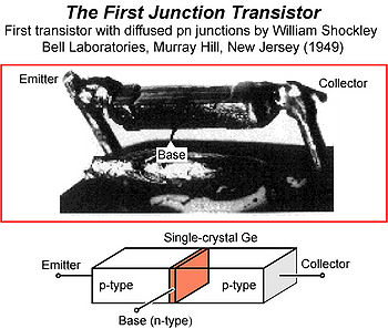
When files were being patented, William's name was not listed in any of them. Although William had contributed as much, or even more, than the others in the group, Julius Lilienfield had not listed his name anywhere. This frustrated and inspired Shockley to create his own transistor. He had withheld some information while working with the Bell Laboratories group and so, he improved upon what they had already worked on. On February 13, 1948, John Shive's invention of using bronze contacts on the point contact transistor inspired Shockley to build the junction transistor. The junction transistor was significantly more durable and consisted of a sandwich structure. This sandwich structure was used by many transistors in the 1960's.
While working on the junction transistor, he had been working on his magnum opus. In it, he included his diode equation, as follows:
- [math]\displaystyle{ I=I_\mathrm{S} \left( e^{V_\mathrm{D}/(n V_\mathrm{T})}-1 \right),\, }[/math]
where
- I is the diode current,
- IS = scale current,
- VD = voltage across the diode,
- VT = thermal voltage, and
- n = ideality factor
William's invention of the junction transistor was announced on July 4th, 1951.
Connectedness
Transistors are one of the most important components in electronic devices. To see the origins of the transistor and its development is something many can appreciate. William's story is very personal as well. From being discredited to inventing a better transistor, William shows the a story of determination, innovation, and perseverance.
History
- Who: William B. Shockley
- What: Junction Transistor
- When: 1949
- Where: Outside of Bell Laboratories
- Why: Majority of transistors in the 1960's used the sandwich structure of the junction transistor
See Also
Further reading
Shockley, William. Electrons and Holes in Semiconductors: With Applications to Transistor Electronics. New York: Van Nostrand, 1950. Print
External links
- Interview with Shockley biographer Joel Shurkin
- History of the transistor
- William Shockley (IEEE Global History Network)
References
First image taken from http://www.nobelprize.org/nobel_prizes/physics/laureates/1956/shockley.jpg Second image take from https://www.ecse.rpi.edu/~schubert/Educational-resources/1949%20First%20junction%20transistor%20(Shockley%20et%20al).jpg